


Research
Research Areas
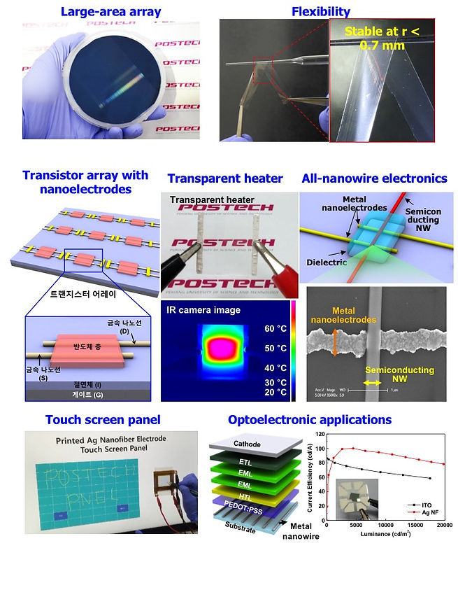
Printed Nano-electronics
Printed Electronics is one of the fastest growing technologies in the World.
Printed and potentially printed electronics is creating many new products given the benefits of the technology compared to conventional electronics, such as thinness, flexibility, cost, ease of manufacture, fast production turn around, "green" technology, power efficiency and more.
Printed electronics is a revolutionary technology aimed at unconventional electronic device manufacture on plastic foils, and will probably rely on polymeric semi-conductors for organic transistor fabrication. In addition to having excellent charge-transport characteristics in the nano electronics

Innovations in nanotechnology promise to revolutionize the forms and functionalities of electronic devices. Offering much more than current technologies on a smaller scale, nanoelectronics researchers apply the unique properties of single particles to change the ways components are powered, manufactured, and used.
-
Robotic Electro-hydrodynamic Nanowire Printing (EHP)
Electrospinningisone of well-known method for fabrication of organic nanowires, which employs the electrostatic force to stretch the polymer solution into nanowire. It’svery simple and fast process to make a very long nanowire.
However,electrospunnanowires are randomly coiled, because of chaotic whipping. It is a serious problem for practical device application. To obtain the aligned nanowires and large-area electronic applications of organic nanowires, we develop a novel process, called electro-hydrodynamic nanowire printing (ENP).

-
Organic Nanowire Electronics


When fabricating transistors using organic semiconducting nanowires, forming the wires at the desired positionin an individually controlled fashion is usually very difficult.UsingENP, we can fabricate well-alignedorganic nanowire field-effect transistors (FETs) very simply and quickly.

Another important advantage of ENP is that the number of aligned nanowires can be easily controlled. the maximum on-current level increased linearly with the number of wires in FETs. This relationship indicates that device characteristics can be precisely controlled by adjusting the number of wires with the ENP technique.


Using ENP technique, we can fabricate the large-area organic nanowire FETs array on a flexible substrate.

[References]
1. Nature Commun.(2013) 4, 1773
2. Advanced Materials (2014), 26, 21, 3459
3. Science Advances (2016), 2, e1501326
4. Advanced Optical Materials (2016), 4, 967
5. Advanced Materials (2014), 26, 47, 8010
6. Advanced Materials (2016), 28, 3, 527